| CPC H10K 59/123 (2023.02) [H10K 59/1213 (2023.02); H10K 59/131 (2023.02); H10K 77/111 (2023.02); H10K 2102/311 (2023.02)] | 13 Claims |
|
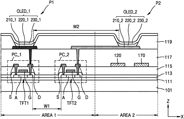
1. A display device comprising:
a substrate comprising a first area and a second area adjacent to the first area;
pixel circuits disposed on the substrate, and the pixel circuits comprising a first pixel circuit disposed in the first area and a second pixel circuit disposed in the first area; and
display elements disposed on the substrate, the display elements comprising:
a first display element disposed in the first area and electrically connected to the first pixel circuit, wherein the first pixel circuit and the display element are disposed to overlap each other on the substrate; and
a second display element disposed in the second area and electrically connected to the second pixel circuit,
wherein the second display element is configured not to overlap the second pixel circuit.
|