| CPC H10K 59/122 (2023.02) [H10K 50/11 (2023.02); H10K 50/81 (2023.02); H10K 50/813 (2023.02); H10K 50/82 (2023.02); H10K 50/84 (2023.02); H10K 59/1213 (2023.02); H10K 59/35 (2023.02); H10K 59/353 (2023.02); H10K 59/38 (2023.02); H10K 50/856 (2023.02); H10K 59/124 (2023.02); H10K 59/352 (2023.02)] | 20 Claims |
|
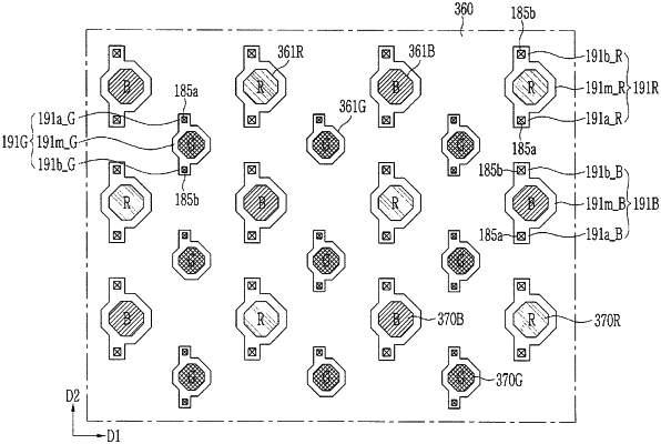
1. A display device, comprising:
a substrate;
a first thin film transistor on the substrate;
a first electrode on the thin film transistor; and
a first emission layer on the first electrode,
wherein the first electrode includes:
a first emission region;
a first contact region protruding from the first emission region in a first direction in a plan view and overlapping a first contact hole through which the first electrode electrically connecting the first thin film transistor; and
a first dummy region protruding from the first emission region in a second direction opposite to the first direction with the first emission region between the first contact region and the first dummy region in a plan view, wherein
the first emission layer overlaps the first emission region of the first electrode.
|