| CPC H10K 59/122 (2023.02) [C23C 14/042 (2013.01); H10K 50/822 (2023.02); H10K 50/828 (2023.02); H10K 71/00 (2023.02); H10K 59/121 (2023.02); H10K 2102/351 (2023.02)] | 1 Claim |
|
1. A method for manufacturing a display backplane, comprising:
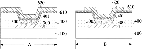
forming a first insulating layer and an emitting layer on a side of a substrate, wherein a transparent display area and a normal display area are divided on the substrate, the first insulating layer has a plurality of openings, and an orthographic projection of the openings on the substrate is within an orthographic projection of the emitting layer on the substrate;
forming a first sub-layer of a first electrode on a remote side of the emitting layer and a remote side of the first insulating layer from the substrate; and
forming a second sub-layer of the first electrode on a remote surface of the first sub-layer from the substrate, wherein the second sub-layer is patterned by a vapor deposition using a second mask defining a second opening portion and a fine metal mask portion, and an opening shape of the second opening portion corresponds to a shape of the second sub-layer in the normal display area, and a hollowed-out pattern of the fine metal mask portion corresponds to a shape of the second sub-layer in the transparent display area,
wherein a thickness of the first sub-layer is smaller than a thickness of the second sub-layer.
|