| CPC H10K 50/8445 (2023.02) [H10K 59/123 (2023.02); H10K 59/124 (2023.02); H10K 59/1213 (2023.02); H10K 59/131 (2023.02)] | 20 Claims |
|
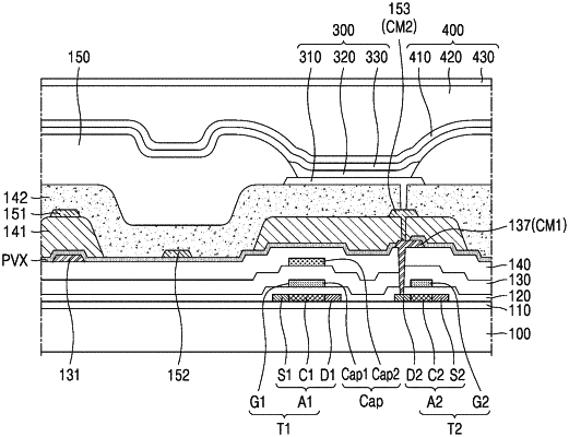
1. A display device comprising:
a substrate comprising a display area and a peripheral area;
a thin film transistor arranged on the substrate;
a first metal wiring layer electrically connected to the thin film transistor;
an inorganic protective layer on the first metal wiring layer;
a patterned first organic film layer located on the inorganic protective layer and overlapping the first metal wiring layer in a plan view;
a second metal wiring layer on the first organic film layer; and
a second organic film layer on the second metal wiring layer,
wherein the first organic film layer is patterned to be arranged at a position where the first metal wiring layer and the second metal wiring layer overlap each other in the plan view, and is not arranged on an entirety of the display area,
the second organic film layer is arranged on the entire display area, and
at least a portion of the second organic film layer contacts an upper surface of the inorganic protective layer.
|