| CPC H10K 39/32 (2023.02) [H01L 27/146 (2013.01); H01L 27/14669 (2013.01)] | 20 Claims |
|
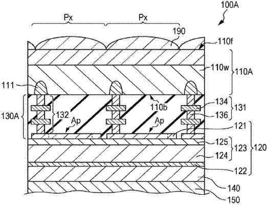
1. An imaging device comprising:
a semiconductor substrate including a first surface that receives light from outside, and a second surface opposite to the first surface;
a first transistor located on the second surface; and
a photoelectric converter that faces the second surface and that receives light transmitted through the semiconductor substrate, wherein
the semiconductor substrate is a silicon substrate or a silicon compound substrate,
the photoelectric converter includes
a first electrode electrically connected to the first transistor,
a second electrode, and
a photoelectric conversion layer that is located between the first electrode and the second electrode and that contains a material which absorbs light having a first wavelength longer than or equal to 1.1 μm, and
the material has a quantum nanostructure.
|