| CPC H10K 39/32 (2023.02) [H01L 27/14612 (2013.01); H01L 27/14636 (2013.01); H01L 27/14643 (2013.01); H01L 27/1463 (2013.01); H01L 27/14689 (2013.01); H10K 30/82 (2023.02)] | 20 Claims |

|
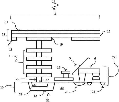
1. A sensor, said sensor comprising:
an array of pixels;
at least one pixel in said array comprising a photodiode structure built on top of an integrated circuit generating a charge;
said integrated circuit comprising at least one semiconductor material and at least one interconnect layer;
said at least one interconnect layer comprising an interconnect to facilitate said charge flowing into a collection node disposed in said semiconductor material;
said interconnect being in contact with a doped contact diffusion disposed within said collection node;
a transfer transistor disposed between said collection node and a conversion node, said conversion node coupled to an active transistor;
each said at least one pixel having a reset configured to reset said conversion node;
at least one bias circuit providing bias to said array;
at least one clock circuit providing clocking to said array; and
at least one signal chain circuit detecting a signal output by at least one pixel of said array.
|