| CPC H10B 63/84 (2023.02) [H10N 70/063 (2023.02)] | 20 Claims |
|
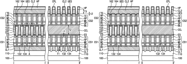
1. A three-dimensional (3D) semiconductor memory device, comprising:
first cell stacks arranged in a first direction and a second direction which are parallel to a top surface of a substrate and intersect each other,
second cell stacks disposed on the first cell stacks and arranged in the first direction and the second direction;
first conductive lines extending in the first direction and provided between the substrate and the first cell stacks;
common conductive lines extending in the second direction and provided between the first cell stacks and the second cell stacks;
etch stop patterns extending in the second direction and provided between the common conductive lines and top surfaces of the first cell stacks, the etch stop patterns including a conductive material;
second conductive lines extending in the first direction and provided on the second cell stacks; and
a capping pattern covering sidewalls of the common conductive lines and sidewalls of the etch stop patterns,
wherein each of the common conductive lines has a second thickness greater than a first thickness of each of the first conductive lines.
|