| CPC H10B 63/32 (2023.02) [H10B 63/80 (2023.02)] | 20 Claims |
|
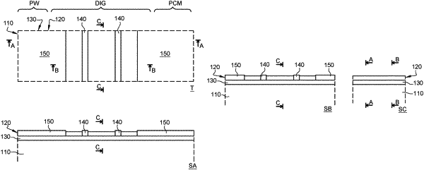
1. A method for manufacturing an electronic chip, comprising:
oxidizing a plurality of first portions and a plurality of second portions of a semiconductor layer down to an insulator, the insulator covering a semiconductor substrate, the semiconductor layer disposed on the insulator;
generating stresses in third portions of the semiconductor layer, each of the third portions extending between two portions of any of the first or second portions of the semiconductor layer; and
forming cavities extending at least to the substrate through the second portions and the insulator.
|