US 11,723,219 B2
Semiconductor structure and manufacturing method of the same
Harry-Hak-Lay Chuang, Paya Lebar Crescent (SG); Sheng-Huang Huang, Hsinchu (TW); Keng-Ming Kuo, Yunlin County (TW); and Hung Cho Wang, Taipei (TW)
Assigned to TAIWAN SEMICONDUCTOR MANUFACTURING COMPANY LTD., Hsinchu (TW)
Filed by TAIWAN SEMICONDUCTOR MANUFACTURING COMPANY LTD., Hsinchu (TW)
Filed on Apr. 29, 2021, as Appl. No. 17/244,768.
Application 17/244,768 is a division of application No. 16/884,883, filed on May 27, 2020, granted, now 10,998,377.
Application 16/884,883 is a division of application No. 15/962,434, filed on Apr. 25, 2018, granted, now 10,727,272, issued on Jul. 28, 2020.
Claims priority of provisional application 62/590,465, filed on Nov. 24, 2017.
Prior Publication US 2021/0249471 A1, Aug. 12, 2021
Int. Cl. H01L 27/22 (2006.01); H01L 43/12 (2006.01); H10B 61/00 (2023.01); H10N 50/01 (2023.01); H10N 50/10 (2023.01); H10N 50/80 (2023.01)
CPC H10B 61/22 (2023.02) [H10N 50/01 (2023.02); H10N 50/10 (2023.02); H10N 50/80 (2023.02)] 20 Claims
OG exemplary drawing
 
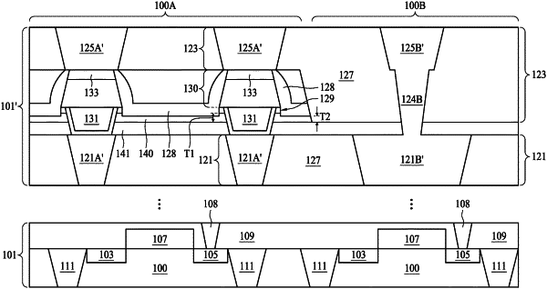
1. A semiconductor structure, comprising:
a memory region;
a logic region adjacent to the memory region;
a first magnetic tunneling junction (MTJ) cell and a second MTJ cell over the memory region;
a carbon-based layer over the memory region, wherein the carbon-based layer comprises a recess between the first MTJ cell and the second MTJ cell; and
a bottom electrode via under the first MTJ cell, wherein an uppermost surface of the bottom electrode via is above an uppermost surface of the carbon-based layer.