US 11,723,218 B2
Semiconductor device and method for forming the same
Shy-Jay Lin, Jhudong Township (TW); Chien-Min Lee, Hsinchu (TW); Hiroki Noguchi, Hsinchu (TW); Mingyuan Song, Hsinchu (TW); Yen-Lin Huang, Hsinchu (TW); and William Joseph Gallagher, Hsinchu (TW)
Assigned to TAIWAN SEMICONDUCTOR MANUFACTURING COMPANY, LTD., Hsinchu (TW)
Filed by Taiwan Semiconductor Manufacturing Co., Ltd., Hsinchu (TW)
Filed on Mar. 29, 2021, as Appl. No. 17/216,162.
Claims priority of provisional application 63/045,285, filed on Jun. 29, 2020.
Prior Publication US 2021/0408115 A1, Dec. 30, 2021
Int. Cl. H01L 21/00 (2006.01); H10B 61/00 (2023.01); H01L 23/528 (2006.01); H01L 21/768 (2006.01); H01L 21/8234 (2006.01)
CPC H10B 61/22 (2023.02) [H01L 21/76898 (2013.01); H01L 21/823475 (2013.01); H01L 23/528 (2013.01)] 20 Claims
OG exemplary drawing
 
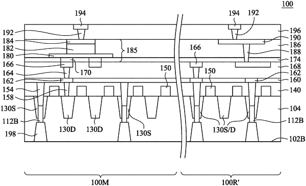
1. A device comprising:
a substrate having a first side and a second side; and
a memory device, comprising:
a transistor disposed over the first side of the substrate, wherein the transistor comprises a gate and a source feature and a drain feature interposing the gate;
first conductive lines disposed over the transistor;
a memory stack disposed over the first conductive lines; and
second conductive lines disposed over the second side of the substrate, wherein at least one of the second conductive lines is a source line or a word line of the memory device.