US 11,723,215 B2
Semiconductor device and method for fabricating the same
Da-Jun Lin, Kaohsiung (TW); Yi-An Shih, Changhua County (TW); Bin-Siang Tsai, Changhua County (TW); and Fu-Yu Tsai, Tainan (TW)
Assigned to UNITED MICROELECTRONICS CORP., Hsin-Chu (TW)
Filed by UNITED MICROELECTRONICS CORP., Hsin-Chu (TW)
Filed on Nov. 30, 2020, as Appl. No. 17/106,214.
Claims priority of application No. 202011203268.7 (CN), filed on Nov. 2, 2020.
Prior Publication US 2022/0140002 A1, May 5, 2022
Int. Cl. H10B 61/00 (2023.01); H10N 50/01 (2023.01); H10N 50/80 (2023.01)
CPC H10B 61/00 (2023.02) [H10N 50/01 (2023.02); H10N 50/80 (2023.02)] 7 Claims
OG exemplary drawing
 
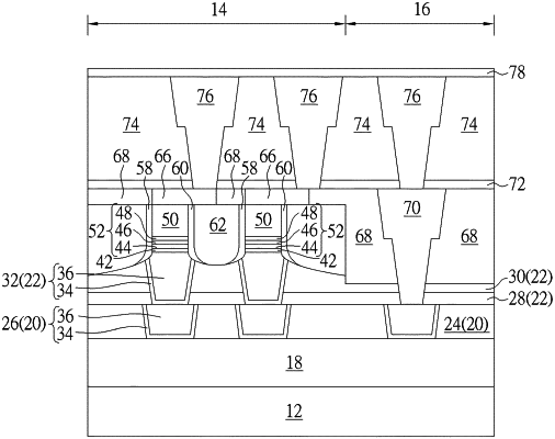
1. A semiconductor device, comprising:
a magnetic tunneling junction (MTJ) on a substrate;
a top electrode on the MTJ;
a first inter-metal dielectric (IMD) layer around the top electrode and the MTJ, wherein a top surface of the first IMD layer is even with a top surface of the top electrode; and
a landing pad on the top electrode and the first IMD layer, wherein a sidewall of the landing pad is aligned with a sidewall of the top electrode.