| CPC H10B 53/50 (2023.02) [G11C 11/22 (2013.01); G11C 11/56 (2013.01); H10B 53/30 (2023.02); G11C 11/5657 (2013.01); H10B 51/00 (2023.02)] | 14 Claims |
|
1. A method for fabricating an electronic device comprising a semiconductor memory, the method comprising:
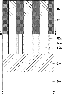
forming a plurality of stacked structures extending in a first direction over a substrate, each of the stacked structures including a first line and an initial memory cell;
forming first liner layers over both sidewalls of the stacked structure in a second direction crossing the first direction;
forming a first insulating layer between the first liner layers;
forming a plurality of second lines extending in the second direction over the stacked structures, the first liner layers and the first insulating layer;
etching the initial memory cell, the first liner layers, and the first insulating layer exposed by the second lines to form memory cells, first liner layer patterns, and first insulating layer patterns;
forming second liner layers over both sidewalls of each of the memory cells, each of the first liner layer patterns, and each of the first insulating layer patterns in the first direction;
forming a second insulating layer between the second liner layers; and
forming a hole for removing a portion of the second liner layer between the memory cells in the second direction to form a plurality of second liner layer patterns separated from each other in the second direction.
|