| CPC H10B 53/30 (2023.02) [H01L 28/60 (2013.01)] | 20 Claims |
|
14. An integrated circuit, comprising:
a semiconductor substrate;
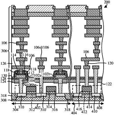
an interconnect structure disposed over an upper surface of the semiconductor substrate, the interconnect structure comprising: a bottommost metal layer, a plurality of inter-metal layers disposed at different heights over the bottommost metal layer, and a plurality of top metal layers disposed at different heights over the inter-metal layers, and a bond pad layer disposed over the plurality of top metal layers; wherein each of the plurality of top metal layers has a width and a thickness that is greater than a width and a thickness, respectively, of each of the plurality of inter-metal layers; and
a ferroelectric capacitor structure disposed within the interconnect structure, the ferroelectric capacitor structure comprising: a bottom electrode structure disposed over an uppermost inter-metal layer of the plurality of inter-metal layers, a ferroelectric structure over the bottom electrode structure, and a top electrode structure disposed under a lowermost top metal layer of the plurality of top metal layers.
|