| CPC H10B 51/30 (2023.02) [H10B 51/10 (2023.02); H10B 51/20 (2023.02)] | 16 Claims |
|
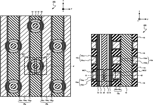
1. A semiconductor memory device, comprising:
a first gate electrode layer extending in a first direction;
a second gate electrode layer extending in the first direction, and the second gate electrode layer spaced from the first gate electrode layer in a second direction orthogonal to the first direction;
a semiconductor layer provided between the first gate electrode layer and the second gate electrode layer, a longitudinal direction of the semiconductor layer extending in a third direction orthogonal to the first direction and the second direction; and
a dielectric layer surrounding the semiconductor layer, the dielectric layer containing oxygen and at least one of hafnium or zirconium, the dielectric layer including a first region containing at least one crystal of an orthorhombic crystal system or a trigonal crystal system as a main component substance, the first region provided between the first gate electrode layer and the semiconductor layer, the dielectric layer including a second region containing at least one crystal of the orthorhombic crystal system or the trigonal crystal system as a main component substance, the second region provided between the second gate electrode layer and the semiconductor layer, and the dielectric layer including a third region containing a substance other than the at least one crystal of the orthorhombic crystal system or the trigonal crystal system as a main component substance, the third region provided between the first region and the second region.
|