| CPC H10B 43/40 (2023.02) [G11C 7/18 (2013.01); G11C 16/08 (2013.01); H10B 41/10 (2023.02); H10B 41/27 (2023.02); H10B 41/35 (2023.02); H10B 41/41 (2023.02); H10B 43/10 (2023.02); H10B 43/27 (2023.02); H10B 43/35 (2023.02)] | 17 Claims |
|
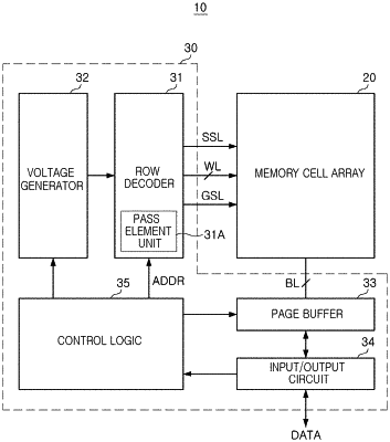
1. A memory device, comprising:
a peripheral circuit region including a row decoder and a page buffer; and
a cell region including a plurality of wordlines stacked to each other, a plurality of channel structures penetrating the plurality of wordlines, and a plurality of cell contacts connected to the plurality of wordlines, the plurality of cell contacts are disposed in a first cell contact region and a second cell contact region,
wherein the first cell contact region and the second cell contact region are disposed on both sides of the plurality of channel structures, in a first direction,
the cell region and the peripheral circuit region are stacked in a vertical direction in which the plurality of channel structures are extended,
each of the first cell contact region and the second cell contact region has a plurality of first pads and a plurality of second pads,
in the first direction, a length of each of the plurality of first pads is shorter than a length of each of the plurality of second pads, and
an area of at least one of the plurality of second pads included in the first cell contact region is greater than an area of at least one of the plurality of second pads included in the second cell contact region.
|