| CPC H10B 43/27 (2023.02) [G11C 13/0004 (2013.01); G11C 13/0069 (2013.01); G11C 16/0483 (2013.01); G11C 16/10 (2013.01); H10B 41/27 (2023.02); H10B 63/34 (2023.02); H10B 63/845 (2023.02); H10N 70/231 (2023.02); G11C 2213/75 (2013.01)] | 11 Claims |
|
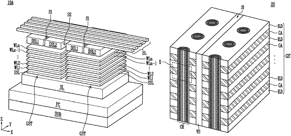
1. A method of manufacturing a semiconductor memory device, the method comprising:
forming a stack structure by alternately stacking a plurality of interlayer insulating layer and a plurality of sacrificial layers on a substrate;
forming a plurality of holes penetrating the stack structure in a vertical direction; and
sequentially forming a blocking insulating layer, a charge storage layer, an emission preventing layer, a tunnel insulating layer, and a channel layer on a sideman of each of the plurality of holes.
|