| CPC H10B 43/27 (2023.02) [H01L 23/535 (2013.01); H10B 41/10 (2023.02); H10B 41/27 (2023.02); H10B 41/35 (2023.02); H10B 41/41 (2023.02); H10B 41/50 (2023.02); H10B 43/10 (2023.02); H10B 43/35 (2023.02); H10B 43/40 (2023.02); H10B 43/50 (2023.02); H10B 63/34 (2023.02); H10B 63/845 (2023.02); H10N 70/231 (2023.02)] | 6 Claims |
|
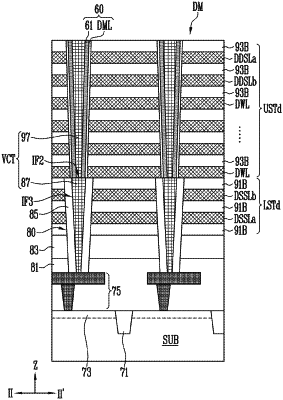
1. A method of manufacturing a semiconductor memory device, the method comprising:
forming a lower stack structure on a substrate with a first region and a second region;
forming a first slit and a lower contact hole that penetrate the lower stack structure, the first slit overlapping with the first region, the lower contact hole overlapping with the second region;
forming an isolation insulating layer that fills the first slit;
forming a first sidewall insulating layer that covers a sidewall of the lower contact hole during the forming of the isolation insulating layer;
forming a first contact pattern on the first sidewall insulating layer to fill the lower contact hole;
forming an upper stack structure on the lower stack structure, the upper stack structure extending to cover the isolation insulating layer and the first contact pattern;
forming channel structures that penetrates the upper stack structure and the lower stack structure, the channel structures overlapping with the first region; and
forming a second contact pattern that penetrates the upper stack structure, overlapping with the second region, the second contact pattern being connected to the first contact pattern.
|