| CPC H10B 43/27 (2023.02) [H10B 43/10 (2023.02); H10B 43/40 (2023.02); H10B 43/50 (2023.02)] | 20 Claims |
|
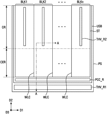
1. A semiconductor memory device, comprising:
a peripheral logic structure including a peripheral circuit and a lower connection wiring body on a substrate;
a horizontal conductive substrate on the peripheral logic structure;
a stacked structure including a plurality of electrode pads stacked in a vertical direction on the horizontal conductive substrate;
a plate contact plug connected to the horizontal conductive substrate, extending in the vertical direction, and disposed in a first region extending in a first horizontal direction orthogonal to the vertical direction;
a first penetration electrode connected to the lower connection wiring body, extending in the vertical direction, and disposed in a second region extending in the first horizontal direction, and
a second penetration electrode penetrating the stacked structure, connected to the lower connection wiring body, and disposed in a third region extending in the vertical direction and a second horizontal direction perpendicular to the first horizontal direction and the vertical direction;
wherein:
an upper surface of the plate contact plug and an upper surface of the first penetration electrode are on a same plane,
the plate contact plug includes an upper part and a lower part directly connected to each other,
the first penetration electrode includes an upper part and a lower part directly connected to each other,
moving away from the upper surface of the first penetration electrode in the vertical direction, a width of the upper part of the first penetration electrode increases, as measured in the second horizontal direction,
moving away from the upper surface of the plate contact plug in the vertical direction, a width of the upper part of the plate contact plug increases, as measured in the second horizontal direction,
moving away from the upper surface of the plate contact plug in the vertical direction, a width of the lower part of the plate contact plug decreases, as measured in the second horizontal direction, and
moving away from the upper surface of the first penetration electrode, a width of the lower part of the first penetration electrode decreases, as measured in the second horizontal direction.
|