| CPC H10B 43/20 (2023.02) [G11C 7/18 (2013.01); H01L 29/0649 (2013.01); H01L 29/0847 (2013.01)] | 20 Claims |
|
1. A semiconductor device comprising:
a first substrate including a cell region and an extension region surrounding the cell region;
a common source plate disposed on the first substrate;
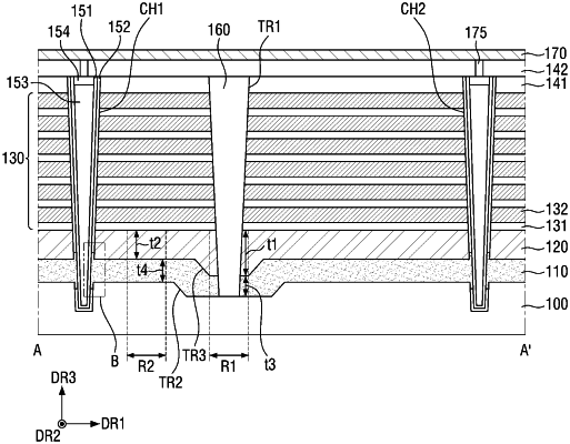
a supporter disposed on the common source plate;
a stack structure disposed on the supporter and including insulating films and gate electrodes alternately stacked;
a channel hole penetrating the stack structure, the supporter, and the common source plate on the cell region of the first substrate;
an electrode isolation trench spaced apart from the channel hole in a first direction on the cell region of the first substrate, extending lengthwise in a second direction perpendicular to the first direction, and penetrating the stack structure, the supporter, and the common source plate; and
a transistor overlapping the stack structure in a third direction perpendicular to the first and second directions,
wherein a first thickness of the supporter in a first region adjacent to the electrode isolation trench in the first direction is greater than a second thickness of the supporter in a second region formed between the electrode isolation trench and the channel hole.
|