| CPC H10B 43/20 (2023.02) [H10B 43/30 (2023.02); H10B 51/20 (2023.02); H10B 51/30 (2023.02)] | 20 Claims |
|
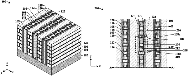
1. A memory device, comprising:
a substrate;
a stack of gate electrode layers, wherein the stack of gate electrode layers is arranged over the substrate;
interconnect dielectric layers arranged above and below each gate electrode layer of the stack of gate electrode layers;
a first memory cell arranged over the substrate and comprising:
a first source/drain conductive line extending vertically through the stack of gate electrode layers;
a second source/drain conductive line extending vertically through the stack of gate electrode layers;
a first barrier structure arranged between a first side of the first source/drain conductive line and a first side of the second source/drain conductive line;
a first protective liner layer arranged directly between the first side of the first source/drain conductive line and the first barrier structure and arranged directly between the first side of the second source/drain conductive line and the first barrier structure;
a channel layer arranged on outermost sidewalls of the first protective liner layer and extending between the first source/drain conductive line and the second source/drain conductive line;
a memory layer arranged on outermost sidewalls of the channel layer;
a second barrier structure on a second side opposite to the first side of the first source/drain conductive line; and
a second protective liner layer arranged directly between the second barrier structure and the second side of the first source/drain conductive line.
|