| CPC H10B 43/20 (2023.02) [H10B 41/10 (2023.02); H10B 41/20 (2023.02); H10B 41/35 (2023.02); H10B 43/10 (2023.02); H10B 43/35 (2023.02)] | 10 Claims |
|
1. A method for manufacturing a semiconductor device, comprising:
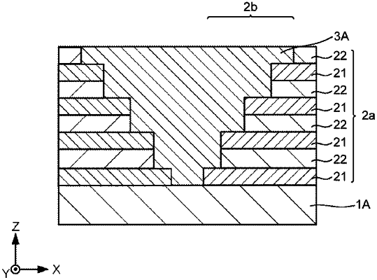
alternately stacking a first film and a second film on an object to form a multilayer film stack;
forming a stacked body and a recess by removing portions of the multilayer film stack;
forming a dielectric layer by applying a composite material to the recess such that the recess is filled with the dielectric layer, the composite material comprising an inorganic material and an organic material;
exposing the dielectric layer to an oxidizing gas to oxidize the inorganic material and to remove at least part of the organic material from the dielectric layer.
|