| CPC H10B 41/35 (2023.02) [H01L 21/046 (2013.01); H01L 21/0415 (2013.01); H01L 21/265 (2013.01); H01L 21/823418 (2013.01); H01L 29/42328 (2013.01); H01L 29/66825 (2013.01); H01L 29/788 (2013.01); H10B 41/00 (2023.02); H10B 41/27 (2023.02); H01L 29/7881 (2013.01)] | 5 Claims |
|
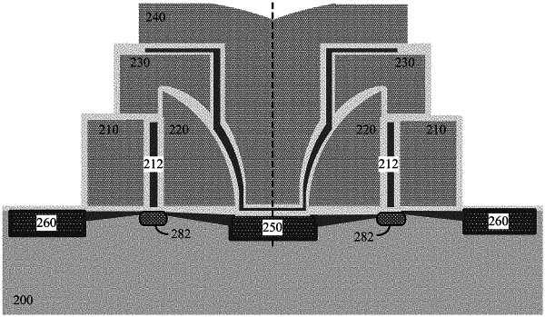
1. A semiconductor structure of a split gate flash memory cell, the split gate flash memory cell comprising at least a select gate and a floating gate formed on a substrate, wherein a side of the select gate is formed with an isolation wall, the floating gate is on the other side of the isolation wall, and an ion implantation region is formed in an upper portion of the substrate below the isolation wall, wherein
an ion implantation type of the ion implantation region is different from an ion implantation type of the substrate,
wherein a source/drain ion implantation region of the split gate flash memory cell is formed in an upper portion of the substrate on the other side of the select gate and an upper portion of the substrate on the other side of the floating gate, wherein the depth of the ion implantation region is smaller than the depth of the source/drain ion implantation region.
|