US 11,723,195 B2
Semiconductor device having an inter-layer via (ILV), and method of making same
Tsung-Hsien Huang, Hsinchu (TW); Hong-Chen Cheng, Hsinchu (TW); Hung-Jen Liao, Hsinchu (TW); and Cheng Hung Lee, Hsinchu (TW)
Assigned to TAIWAN SEMICONDUCTOR MANUFACTURING COMPANY, LTD., Hsinchu (TW)
Filed by TAIWAN SEMICONDUCTOR MANUFACTURING COMPANY, LTD., Hsinchu (TW)
Filed on May 20, 2021, as Appl. No. 17/325,708.
Application 17/325,708 is a division of application No. 16/205,751, filed on Nov. 30, 2018, granted, now 11,024,634.
Application 16/205,751 is a division of application No. 15/333,439, filed on Oct. 25, 2016, granted, now 10,170,487, issued on Jan. 1, 2019.
Application 15/333,439 is a continuation of application No. 14/039,481, filed on Sep. 27, 2013, granted, now 9,484,350, issued on Nov. 1, 2016.
Prior Publication US 2021/0272968 A1, Sep. 2, 2021
Int. Cl. H01L 27/112 (2006.01); G11C 7/18 (2006.01); H10B 20/00 (2023.01); H01L 23/522 (2006.01); H01L 21/768 (2006.01); H01L 23/528 (2006.01); H01L 27/06 (2006.01)
CPC H10B 20/50 (2023.02) [G11C 7/18 (2013.01); H01L 21/76816 (2013.01); H01L 21/76877 (2013.01); H01L 23/5226 (2013.01); H01L 23/5283 (2013.01); H01L 27/0688 (2013.01); H01L 2924/0002 (2013.01)] 20 Claims
OG exemplary drawing
 
1. A method of making a semiconductor device, the method comprising:
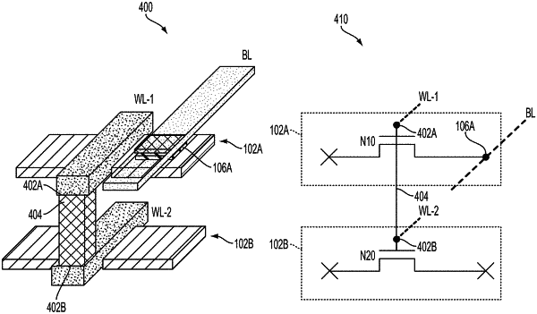
forming a first memory device;
connecting a first word line to the first memory device;
forming at least a first via;
forming a second memory device, wherein the first and second memory devices are separated by an inter-layer dielectric (ILD), and the first via connects the first memory device and the second memory device;
connecting a second word line to the second memory device;
connecting a bit line to the first memory device,
wherein the first word line is connected to the second word line by the first via, and the first via is directly connected to at least the first word line.