| CPC H10B 12/34 (2023.02) [H10B 12/0335 (2023.02); H10B 12/053 (2023.02); H10B 12/315 (2023.02)] | 20 Claims |
|
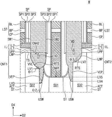
1. A semiconductor memory device comprising:
a substrate comprising a first active pattern, the first active pattern comprising a first source/drain region and a second source/drain region;
a gate electrode crossing the first active pattern, extending in a first direction, and crossing a region between the first and second source/drain regions;
a bit line crossing the first active pattern and extending in a second direction, the bit line being electrically connected to the first source/drain region;
a spacer on a side surface of the bit line;
a first contact coupled to the second source/drain region and spaced apart from the bit line with the spacer interposed therebetween;
a landing pad on the first contact;
a data storing element on the landing pad; and
a conductive pattern between the bit line and the first active pattern,
wherein the second source/drain region has a top surface, an upper side surface, and a curved top surface that extends from the top surface to the upper side surface,
wherein the first contact is in contact with the curved top surface and the upper side surface,
wherein the conductive pattern is coupled to the first source/drain region of the first active pattern,
wherein a bottom surface of the conductive pattern is confined to a planar surface of the first source/drain region, and
wherein the bottom surface of the conductive pattern in contact with the planar surface of the first source/drain region is higher than a lowermost level of the first contact.
|