| CPC H10B 12/315 (2023.02) [H01L 28/75 (2013.01); H01L 28/91 (2013.01); H10B 12/0335 (2023.02)] | 16 Claims |
|
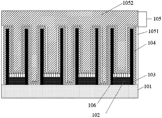
1. A capacitor structure, comprising:
a substrate;
a first capacitor contact layer, arranged directly on the substrate in an array manner;
a bottom electrode layer, surrounding a side wall of the first capacitor contact layer and extending in a direction of the first capacitor contact layer away from the substrate;
a capacitor dielectric layer, covering an upper surface of the substrate, a surface of the bottom electrode layer and an upper surface of the first capacitor contact layer;
a top electrode layer, covering a surface of the capacitor dielectric layer; and
a second capacitor contact layer located at the upper surface of the first capacitor contact layer, the capacitor dielectric layer covering and directly contacting the upper surface of the substrate, the surface of the bottom electrode layer and an upper surface of the second capacitor contact layer;
wherein a material of the first capacitor contact layer is different from a material of the second capacitor contact layer, and the material of the second capacitor contact layer is the same as a material of the bottom electrode layer.
|