| CPC H10B 12/315 (2023.02) [H01L 21/76808 (2013.01); H01L 21/76843 (2013.01); H01L 23/5226 (2013.01); H01L 28/91 (2013.01); H10B 12/033 (2023.02); H10B 12/50 (2023.02)] | 16 Claims |
|
1. An embedded dynamic random access memory (DRAM) device, comprising:
a dielectric layer having a logic area and a memory area, the dielectric layer having an uppermost surface;
a metal trace and a metal via in the logic area of the dielectric layer; and
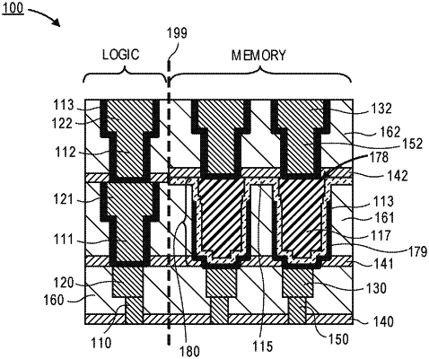
one or more ferroelectric capacitors in the memory area of the dielectric layer, wherein each ferroelectric capacitor includes a first electrode layer, a ferroelectric layer, and a second electrode layer, wherein the ferroelectric layer is between the first electrode layer and the second electrode layer, wherein the ferroelectric layer surrounds the second electrode layer of each ferroelectric capacitor and extends along a top surface of the dielectric layer in the memory area, wherein the ferroelectric layer extends laterally beyond the second electrode layer of each ferroelectric capacitor, wherein the ferroelectric layer has an uppermost surface at a same level as an uppermost surface of the second electrode layer, and wherein the first electrode layer has an uppermost surface below the uppermost surface of the dielectric layer.
|