| CPC H10B 12/30 (2023.02) [G11C 11/4023 (2013.01); G11C 11/412 (2013.01); H10B 10/12 (2023.02); H10B 12/02 (2023.02)] | 20 Claims |
|
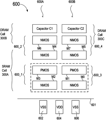
1. A semiconductor device, comprising:
a first stack of transistors positioned over a top surface of a substrate, the first stack of transistors including a first pair of transistors and a second pair of transistors that are stacked over the substrate;
a second stack of transistors positioned over the top surface of the substrate and adjacent to the first stack of transistors, the second stack of transistors including a third pair of transistors and a fourth pair of transistors that are stacked over the substrate;
a first capacitor that is stacked with the first stack of transistors and the second stack of transistors; and
a second capacitor that is positioned adjacent to the first capacitor and stacked with the first stack of transistors and the second stack of the transistors, wherein:
a first group of the transistors in the first stack of transistors and the second stack of transistors are coupled to each other to form a static random-access memory (SRAM) cell, and
a second group of the transistors in the first stack of the transistors and the second stack of transistor are coupled to the first capacitor and the second capacitor to form a first dynamic random-access memory (DRAM) cell and a second DRAM cell that are stacked with and coupled to the SRAM cell.
|