| CPC H10B 12/30 (2023.02) [H01L 28/40 (2013.01); H01L 29/0673 (2013.01); H01L 29/7869 (2013.01); H01L 29/78618 (2013.01); H01L 29/78696 (2013.01); H10B 12/03 (2023.02); H10B 12/05 (2023.02); H10B 12/50 (2023.02); H01L 28/86 (2013.01); H01L 29/42392 (2013.01); H10B 12/482 (2023.02); H10B 12/488 (2023.02)] | 24 Claims |
|
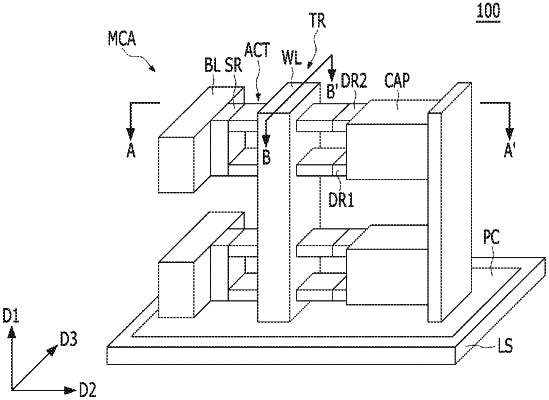
14. A memory device, comprising:
a substrate including a peripheral circuit portion; and
a memory cell array including a plurality of memory cells that are vertically stacked from the peripheral circuit portion,
wherein each of the memory cells includes:
a bit line that is laterally oriented to be parallel to the substrate;
a transistor including two nano sheet channels that are laterally oriented from the bit line and a word line that is vertically oriented and surrounds the two nano sheet channels; and
a capacitor that is laterally oriented from the transistor.
|