| CPC H05K 3/4697 (2013.01) [H05K 3/4007 (2013.01); H05K 3/4038 (2013.01)] | 16 Claims |
|
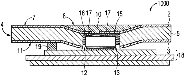
1. A method for manufacturing a circuit carrier, said method comprising:
arranging an electrically conductive first layer on a first side of a board at a distance to a second layer to define an intermediate space there between;
filling the intermediate space with a first insulating material;
curing the board such as to deform a region of the board in such a way that the electrically conductive first layer has an indentation in the deformed region;
forming a cutout on a second side of the board in opposition to the first side such that the indentation and the cut-out lie opposite one another;
structuring the electrically conductive first layer to produce a trace structure;
populating a bare die in the cut-out such as to come into electrical contact with the electrically conductive first layer; and
filling the indentation with a second insulating material.
|