US 11,723,153 B2
Printed circuit board and method of fabricating the same
Yun Mi Bae, Seoul (KR); Soon Gyu Kwon, Seoul (KR); Sang Hwa Kim, Seoul (KR); Sang Young Lee, Seoul (KR); Jin Hak Lee, Seoul (KR); Han Su Lee, Seoul (KR); Dong Hun Jeong, Seoul (KR); In Ho Jeong, Seoul (KR); Dae Young Choi, Seoul (KR); and Jung Ho Hwang, Seoul (KR)
Assigned to LG INNOTEK CO., LTD., Seoul (KR)
Filed by LG INNOTEK CO., LTD., Seoul (KR)
Filed on Mar. 1, 2022, as Appl. No. 17/653,054.
Application 17/653,054 is a continuation of application No. 17/236,519, filed on Apr. 21, 2021, granted, now 11,297,720.
Application 17/236,519 is a continuation of application No. 17/005,522, filed on Aug. 28, 2020, granted, now 11,019,731, issued on May 25, 2021.
Application 17/005,522 is a continuation of application No. 16/717,679, filed on Dec. 17, 2019, granted, now 10,798,827, issued on Oct. 6, 2020.
Application 16/717,679 is a continuation of application No. 15/878,701, filed on Jan. 24, 2018, granted, now 10,531,569, issued on Jan. 7, 2020.
Application 15/878,701 is a continuation of application No. 15/594,778, filed on May 15, 2017, granted, now 9,913,383, issued on Mar. 6, 2018.
Application 15/594,778 is a continuation of application No. 14/831,674, filed on Aug. 20, 2015, granted, now 9,686,860, issued on Jun. 20, 2017.
Claims priority of application No. 10-2015-0100404 (KR), filed on Jul. 15, 2015.
Prior Publication US 2022/0240390 A1, Jul. 28, 2022
Int. Cl. H05K 1/11 (2006.01); H05K 3/24 (2006.01); H05K 3/18 (2006.01); H05K 3/10 (2006.01); H05K 1/02 (2006.01); C25D 3/48 (2006.01); C25D 5/02 (2006.01); C25D 5/48 (2006.01); C25D 7/12 (2006.01); H05K 1/09 (2006.01); C25D 3/38 (2006.01)
CPC H05K 3/244 (2013.01) [C25D 3/48 (2013.01); C25D 5/022 (2013.01); C25D 5/48 (2013.01); C25D 7/123 (2013.01); H05K 1/0296 (2013.01); H05K 1/09 (2013.01); H05K 1/11 (2013.01); H05K 3/108 (2013.01); H05K 3/181 (2013.01); H05K 3/188 (2013.01); C25D 3/38 (2013.01); H05K 2201/0338 (2013.01); H05K 2201/098 (2013.01); H05K 2201/099 (2013.01); H05K 2201/0989 (2013.01); H05K 2203/1184 (2013.01)] 20 Claims
OG exemplary drawing
 
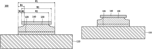
1. A circuit board comprising:
an insulating layer;
a first metal layer disposed on the insulating layer; and
a second metal layer disposed on the first metal layer,
wherein the first metal layer includes:
an upper surface in contact with the second metal layer,
a lower surface facing the insulating layer, and
a side surface disposed between the upper surface and the lower surface
wherein the side surface of the first metal layer includes:
a first side surface connected to the upper surface of the first metal layer and etched inward of the first metal layer; and
a second side surface connecting the first side surface and the lower surface of the first metal layer,
wherein at least a part of the first side surface overlaps the second metal layer in a vertical direction, and
wherein the first side surface has a slope in which a width of the first metal layer changes toward the second side surface of the first metal layer.