| CPC H05K 3/0044 (2013.01) [H05K 3/0026 (2013.01); H05K 3/284 (2013.01); H05K 2203/025 (2013.01)] | 20 Claims |
|
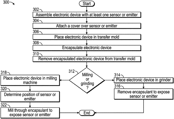
1. A method comprising:
assembling at least one electronic device with a sensor or an emitter;
placing a cover over the sensor or the emitter;
placing the electronic device into a mold cavity of a transfer mold, wherein the mold cavity has a height substantially identical to a height of the cover;
encapsulating the electronic device with an encapsulant, yielding an encapsulated electronic device;
removing the encapsulated electronic device from the transfer mold;
placing the encapsulated electronic device in a milling machine;
determining a position of the sensor or the emitter; and
milling a top portion of the cover to expose the sensor or the emitter based on the position of the sensor or the emitter.
|