| CPC H05K 1/183 (2013.01) [H01L 23/13 (2013.01); H01L 23/49822 (2013.01); H01L 23/49838 (2013.01); H01L 23/642 (2013.01); H01L 25/0657 (2013.01); H05K 1/181 (2013.01); H01L 23/49816 (2013.01); H05K 2201/10015 (2013.01); H05K 2201/10159 (2013.01)] | 7 Claims |
|
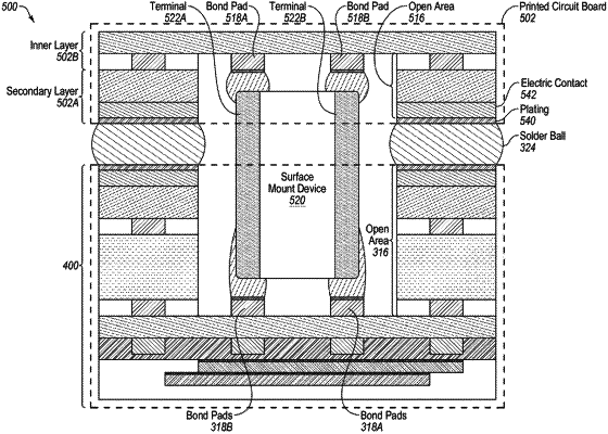
1. An apparatus, comprising:
a primary layer of a substrate comprising a first external surface of the substrate;
a secondary layer of the substrate comprising an open area that extends through the secondary layer to an inner layer of the substrate;
the inner layer of the substrate that is positioned between the primary layer and the secondary layer, wherein the inner layer comprises a first plurality of component bond pads that are disposed on the inner layer and that are exposed via the open area of the secondary layer, wherein a plating material is disposed above the first plurality of component bond pads, and wherein the first plurality of component bond pads comprise sidewalls that are at least in part exposed via the open area of the secondary layer;
a surface mount device comprising a first terminal and a second terminal, wherein the first terminal is coupled to a first component bond pad of the first plurality of component bond pads of the inner layer, and wherein the second terminal is coupled to a second component bond pad of the first plurality of component bond pads of the inner layer; and
a printed circuit board (PCB) comprising an open area that extends through an outer layer of the PCB to an inner layer of the PCB, wherein the inner layer of the PCB comprises a second plurality of component bond pads that are disposed on the inner layer of the PCB; and wherein the first terminal of the surface mount device is coupled to a first component bond pad of the second plurality of component bond pads, and wherein the second terminal of the surface mount device is coupled to a second component bond pad of the second plurality of component bond pads.
|