| CPC H05K 1/111 (2013.01) [G02B 7/006 (2013.01); G02B 7/02 (2013.01); H05K 1/0274 (2013.01); H05K 2201/09409 (2013.01); H05K 2201/09445 (2013.01); H05K 2201/10121 (2013.01); H05K 2201/10151 (2013.01)] | 11 Claims |
|
1. A sensor lens assembly having a non-reflow configuration, comprising:
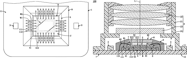
a circuit board having a first surface and a second surface that is opposite to the first surface, wherein the first surface of the circuit board includes a chip-bonding region, a plurality of first soldering pads arranged outside of the chip-bonding region, and a plurality of second soldering pads that are arranged outside of the first soldering pads;
an optical module including:
a frame fixed on the first surface of the circuit board;
at least one lens assembled into the frame, wherein a central axis of the at least one lens passes through the chip-bonding region; and
a filtering sheet assembled into the frame and positioned along the central axis, wherein the frame, the filtering sheet, and the first surface jointly define a distribution space, and the chip-bonding region, the first soldering pads, and the second soldering pads are arranged in the distribution space;
an electronic chip disposed on the chip-bonding region and including a plurality of first connection pads that are arranged on a top side thereof;
a plurality of first wires, wherein the first soldering pads are respectively and electrically coupled to the first connection pads through the first wires;
a sensor chip and a die attach film (DAF), wherein the sensor chip includes a sensing region arranged on a top surface thereof and a plurality of second connection pads that are arranged on the top surface and outside of the sensing region, and the DAF is adhered to a bottom surface of the sensor chip, and wherein the sensor chip is adhered to the top side of the electronic chip through the DAF such that the sensing region is perpendicular to the central axis;
a plurality of second wires, wherein the second soldering pads are respectively and electrically coupled to the second connection pads through the second wires;
a supporting adhesive layer being in a ringed shape and disposed outside of the sensing region; and
a light-permeable sheet, wherein the light-permeable sheet is disposed on the supporting adhesive layer and faces the sensor chip, so that the light-permeable sheet, the supporting adhesive layer, and the top surface of the sensor chip jointly define an enclosed space;
wherein the first soldering pads and the second soldering pads are staggered with respect to each other, respectively.
|