| CPC H04N 25/79 (2023.01) [H04N 23/80 (2023.01); H04N 25/74 (2023.01)] | 18 Claims |
|
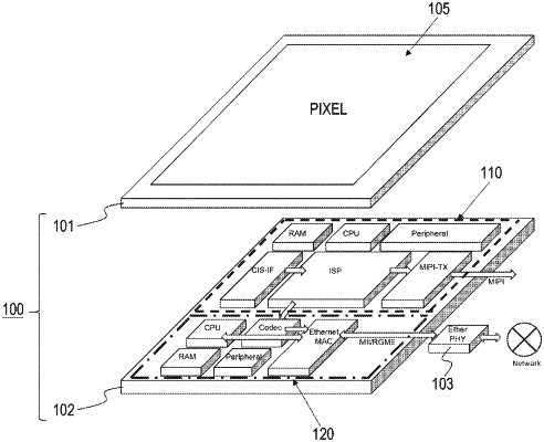
1. An imaging device, comprising:
a plurality of pixels on a first substrate, wherein the plurality of pixels is configured to generate an image signal;
first circuitry on a second substrate stacked on the first substrate, wherein the first circuitry is configured to:
process the image signal to generate a processed image signal; and
output the processed image signal through a first data interface;
second circuitry on the second substrate, wherein the second circuitry is configured to:
encode the processed image signal to generate an encoded compressed signal;
assign an address to the encoded compressed signal to generate an Ethernet frame that includes the encoded compressed signal; and
output the Ethernet frame through a second data interface.
|