US 11,722,800 B2
Semiconductor image sensor module and method of manufacturing the same
Shin Iwabuchi, Kanagawa (JP); and Makoto Motoyoshi, Kanagawa (JP)
Assigned to Sony Group Corporation, Tokyo (JP)
Filed by Sony Group Corporation, Tokyo (JP)
Filed on Dec. 8, 2021, as Appl. No. 17/545,591.
Application 17/545,591 is a continuation of application No. 16/863,383, filed on Apr. 30, 2020, granted, now 11,228,728.
Application 16/863,383 is a continuation of application No. 15/464,959, filed on Mar. 21, 2017, abandoned.
Application 15/464,959 is a continuation of application No. 15/149,534, filed on May 9, 2016, granted, now 10,594,972, issued on Mar. 17, 2020.
Application 15/149,534 is a continuation of application No. 14/193,762, filed on Feb. 28, 2014, granted, now 9,955,097, issued on Apr. 24, 2018.
Application 14/193,762 is a continuation of application No. 11/915,958, granted, now 8,946,610, issued on Feb. 3, 2015, previously published as PCT/JP2006/311007, filed on Jun. 1, 2006.
Claims priority of application No. 2005-163267 (JP), filed on Jun. 2, 2005; and application No. 2005-197730 (JP), filed on Jul. 6, 2005.
Prior Publication US 2022/0124270 A1, Apr. 21, 2022
This patent is subject to a terminal disclaimer.
Int. Cl. H04N 5/378 (2011.01); H01L 27/146 (2006.01); H01L 23/00 (2006.01); H01L 23/48 (2006.01); H01L 25/18 (2023.01); H04N 5/225 (2006.01); H04N 5/369 (2011.01); H04N 5/374 (2011.01); H04N 25/75 (2023.01); H04N 23/54 (2023.01); H04N 25/76 (2023.01); H04N 25/79 (2023.01); H01L 29/788 (2006.01); H01L 29/792 (2006.01); H10B 69/00 (2023.01)
CPC H04N 25/75 (2023.01) [H01L 23/481 (2013.01); H01L 24/16 (2013.01); H01L 25/18 (2013.01); H01L 27/1464 (2013.01); H01L 27/1469 (2013.01); H01L 27/14607 (2013.01); H01L 27/14612 (2013.01); H01L 27/14625 (2013.01); H01L 27/14627 (2013.01); H01L 27/14632 (2013.01); H01L 27/14634 (2013.01); H01L 27/14636 (2013.01); H01L 27/14638 (2013.01); H01L 27/14643 (2013.01); H01L 27/14689 (2013.01); H04N 23/54 (2023.01); H04N 25/76 (2023.01); H04N 25/79 (2023.01); H01L 29/788 (2013.01); H01L 29/792 (2013.01); H01L 2224/0401 (2013.01); H01L 2224/0557 (2013.01); H01L 2224/05552 (2013.01); H01L 2224/05554 (2013.01); H01L 2224/13 (2013.01); H01L 2224/13025 (2013.01); H01L 2224/16145 (2013.01); H01L 2224/16237 (2013.01); H01L 2924/0002 (2013.01); H01L 2924/00014 (2013.01); H01L 2924/13091 (2013.01); H01L 2924/1425 (2013.01); H01L 2924/1436 (2013.01); H01L 2924/1437 (2013.01); H01L 2924/1443 (2013.01); H10B 69/00 (2023.02)] 9 Claims
OG exemplary drawing
 
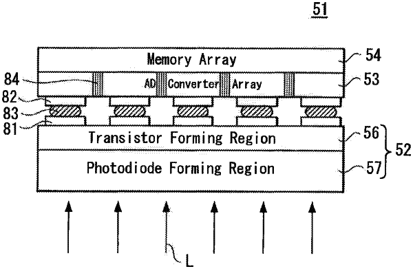
1. An image sensor comprising:
a first semiconductor chip having an image sensor including pixels, each of the pixels including a photoelectric conversion element and transistors; and
a second semiconductor chip including analog/digital converters,
wherein the first semiconductor chip and the second semiconductor chip are stacked and electrically connected to each other.