US 11,722,793 B2
Imaging device and electronic device
Yoshimichi Kumagai, Kanagawa (JP); Takashi Abe, Kanagawa (JP); Ryoto Yoshita, Kanagawa (JP); and Ryo Fukui, Kanagawa (JP)
Assigned to SONY SEMICONDUCTOR SOLUTIONS CORPORATION, Kanagawa (JP)
Filed by SONY SEMICONDUCTOR SOLUTIONS CORPORATION, Kanagawa (JP)
Filed on Apr. 15, 2022, as Appl. No. 17/659,361.
Application 17/659,361 is a continuation of application No. 17/250,392, granted, now 11,330,203, previously published as PCT/JP2019/027260, filed on Jul. 10, 2019.
Claims priority of application No. 2018-138644 (JP), filed on Jul. 24, 2018; and application No. 2018-142341 (JP), filed on Jul. 30, 2018.
Prior Publication US 2022/0311958 A1, Sep. 29, 2022
This patent is subject to a terminal disclaimer.
Int. Cl. H04N 25/53 (2023.01); H04N 25/75 (2023.01); H04N 25/76 (2023.01)
CPC H04N 25/53 (2023.01) [H04N 25/75 (2023.01); H04N 25/76 (2023.01)] 17 Claims
OG exemplary drawing
 
1. An imaging device, comprising:
a plurality of pixels, wherein each pixel of the plurality of pixels includes:
an amplification transistor;
a photoelectric conversion unit;
a holding unit;
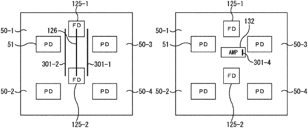
a plurality of floating diffusions shared among the plurality of pixels;
a plurality of boost lines that includes a first boost line and a second boost line, wherein
the first boost line is different from the second boost line, and
the second boost line is in contact with a gate of the amplification transistor; and
an interconnect line configured to connect the plurality of floating diffusions, wherein the interconnect line is parallel to the first boost line.