| CPC H04B 10/503 (2013.01) [H04B 10/40 (2013.01); H04B 10/532 (2013.01)] | 18 Claims |

|
1. A transceiver device comprising:
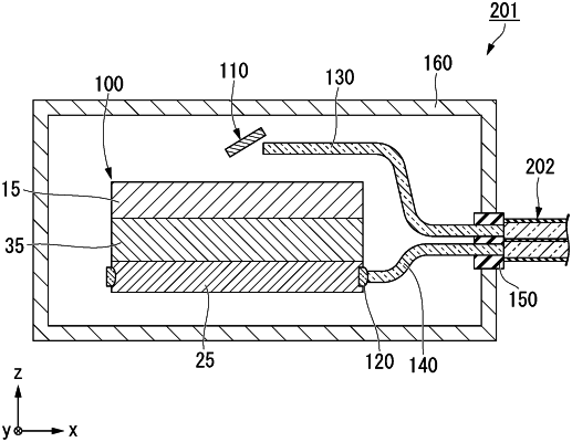
a receiving device including a magnetic element having a first ferromagnetic layer, a second ferromagnetic layer, and a spacer layer sandwiched between the first ferromagnetic layer and the second ferromagnetic layer, the receiving device being configured to receive an optical signal;
a transmission device including a modulated light output element, the transmission device being configured to transmit an optical signal; and
a circuit chip including an integrated circuit electrically connected to the magnetic element and the modulated light output element,
wherein the magnetic element and the modulated light output element are arranged in a direction perpendicular to a surface of the circuit chip, and
a position of the circuit chip in the direction is between a position of the magnetic element in the direction and a position of the modulated light output element in the direction.
|