| CPC H04B 1/0466 (2013.01) [H01Q 1/50 (2013.01); H04B 1/0458 (2013.01)] | 15 Claims |
|
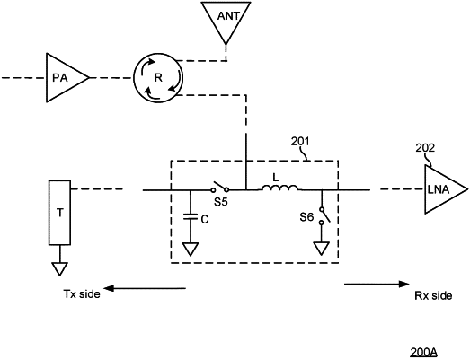
1. A radio frequency (RF) switch circuit for switching RF signals, comprising:
a common port configured to receive an RF signal with a signal frequency;
a first output port and a second output port;
a through switch configured to couple the common port to the second output port in a first mode (TX) of the RF switch circuit and decouple the common port from the second output port in a second mode (RX) of the RF switch circuit;
a shunt switch configured to couple the first output port to a reference potential in the first mode (TX) and decouple of the first output from the reference potential in the second mode (RX);
an inductive element between the common port and the first output port; and
a capacitive element between the second output port and the reference potential, wherein a combination of the inductive element and the capacitive element is configured to resonate at the signal frequency in the first mode (TX) by being connected together by the through switch and by the shunt switch, and combination of the through switch and the shunt switch connecting the inductor and the capacitive element to the reference potential, and
decouple, in the first mode (TX), the common port from the first output port and the second output port from the reference potential thus isolating, in the first mode (TX), the RF signal from the first output port.
|