| CPC H04B 1/04 (2013.01) [H04B 1/0014 (2013.01); H04B 1/667 (2013.01); H04B 2001/0491 (2013.01)] | 18 Claims |
|
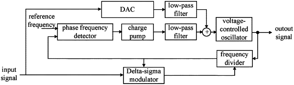
1. A frequency modulation circuit, comprising:
a) a modulation circuit configured to generate a digital modulation signal and an analog modulation signal according to an input signal of the frequency modulation circuit;
b) a phase-locked loop having a voltage-controlled oscillator configured to receive a reference frequency, and to adjust capacitor arrays of the voltage-controlled oscillator according to the analog modulation signal and the digital modulation signal, in order to modulate a frequency of an output signal of the voltage- controlled oscillator; and
c) wherein the capacitor arrays comprises a switched capacitor array and a variable capacitor array, wherein the variable capacitor array comprises variable capacitors, and wherein the capacitance value of the variable capacitor array is adjusted according to low-digit codes of the input signal and an error information between the output signal and the reference frequency.
|