| CPC H03L 7/0992 (2013.01) | 20 Claims |
|
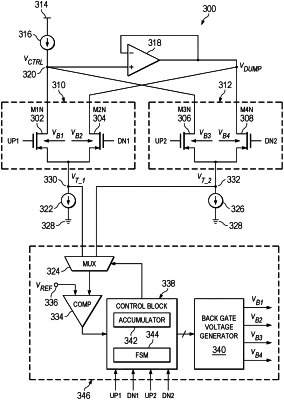
1. A charge pump, comprising:
an output terminal;
a first transistor including a source, a drain, a gate, and a body terminal, the drain of the first transistor coupled to the output terminal;
a second transistor including a source, a drain, a gate, and a body terminal, the drain part of a current path that is separate from a current path that includes the drain of the first transistor;
a control circuit including an output, the control circuit configured to generate a first control signal in response to a voltage at the gate of the first transistor and a voltage at the gate of the second transistor;
a multiplexer (MUX) including a first input, a second input, a control input, and an output, the first input of the MUX coupled to the source of the first transistor and the second input of the MUX coupled to the source of the second transistor, the control input of the MUX coupled to the output of the control circuit;
a reference voltage terminal adapted to receive a reference voltage; and
a calibration circuit including a first input, a second input, a first output and a second output, the first input of the calibration circuit coupled to the output of the MUX, the second input of the calibration circuit coupled to the reference voltage terminal, the first output of the calibration circuit coupled to the body terminal of the first transistor, and the second output of the calibration circuit coupled to the body terminal of the second transistor.
|