| CPC H03K 17/6874 (2013.01) [H04B 1/006 (2013.01); H04B 1/44 (2013.01)] | 16 Claims |
|
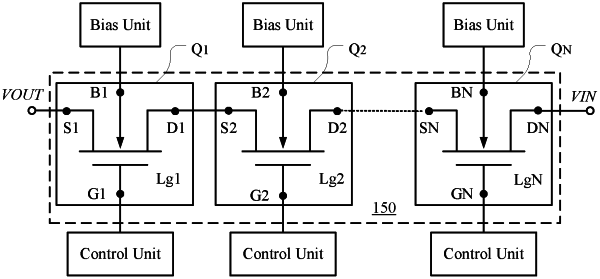
1. A radio frequency switch, comprising:
N switch transistors Q1˜QN connected in series, among which a switch transistor Qi has a first conducting terminal connected to a second conducting terminal of a switch transistor Qi−1, a second conducting terminal of the switch transistor Qi is connected to a first conducting terminal of a switch transistor Qi+1, a first conducting terminal of the switch transistor Q1 serves as an output end of the radio frequency switch, a second conducting terminal of the switch transistor QN serves as an input end of the radio frequency switch, wherein N is an integer greater than 3, i is an integer smaller than N and larger than 1,
wherein for each two adjacent switch transistors of the N switch transistors, one of that two adjacent switch transistors which is located closer to the output end has a higher or equal withstand voltage than that of the other one of that two adjacent switch transistors which is located closer to the input end, or,
for each two adjacent switch transistors of the N switch transistors, one of that two adjacent switch transistors which is located closer to the output end has a lower or equal withstand voltage than that of the other one of that two adjacent switch transistors which is located closer to the input end, or,
wherein a withstand voltage of the switch transistor Q1 is different from a withstand voltage of the switch transistor QN,
wherein the withstand voltage of each one of the N switch transistors is related to its own channel length and/or channel width.
|