| CPC H03K 17/145 (2013.01) [G06F 1/04 (2013.01); H03K 3/037 (2013.01); H03K 21/12 (2013.01)] | 5 Claims |
|
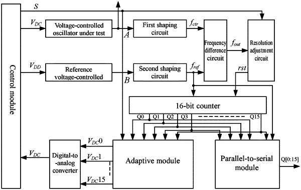
1. An adaptive anti-aging sensor based on a cuckoo algorithm, comprises a control module, a reference voltage-controlled oscillator, two shaping circuits of the same structure, a frequency difference circuit, a resolution adjustment circuit, a 16-bit counter, a parallel-to-serial circuit, an adaptive module and a digital-to-analog converter; the control module has a feedback terminal, a first voltage output terminal, a second voltage output terminal and a control signal output terminal, the reference voltage-controlled oscillator and each of the shaping circuits have an input terminal and an output terminal respectively, the frequency difference circuit has a set terminal, a clock terminal and an output terminal, the resolution adjustment circuit has an input terminal, an output terminal and a control terminal, the 16-bit counter has a set terminal, a reset terminal and 16 bits of parallel output terminals, the adaptive module has a control terminal, 16 bits of parallel input terminals and 16 bits of parallel output terminals, the digital-to-analog converter has 16 bits of parallel input terminals and an output terminal, the parallel-to-serial circuit has a clock terminal, 16 bits of parallel input terminals and an output terminal, the two shaping circuits are referred to as a first shaping circuit and a second shaping circuit respectively, a voltage-controlled oscillator in an integrated circuit is referred to as a voltage-controlled oscillator under test, the reference voltage-controlled oscillator is completely identical with the voltage-controlled oscillator under test, the first voltage output terminal of the control module is used for connecting to an input terminal of the voltage-controlled oscillator under test, the second voltage output terminal of the control module is connected to the input terminal of the reference voltage-controlled oscillator, the control signal output terminal of the control module is connected to the control terminal of the resolution adjustment circuit and the control terminal of the adaptive module respectively, the input terminal of the first shaping circuit is connected to an output terminal of the voltage-controlled oscillator under test, the output terminal of the reference voltage-controlled oscillator is connected to the input terminal of the second shaping circuit, the output terminal of the first shaping circuit is connected to the set terminal of the frequency difference circuit, the output terminal of the second shaping circuit is connected to the clock terminal of the frequency difference circuit, the clock terminal of the parallel-to-serial circuit and the set terminal of the 16-bit counter respectively, the output terminal of the frequency difference circuit is connected to the input terminal of the resolution adjustment circuit, the output terminal of the resolution adjustment circuit is connected to the reset terminal of the 16-bit counter, the 16 bits of parallel output terminals of the 16-bit counter are connected to the 16 bits of parallel input terminals of the parallel-to-serial circuit and the 16 bits of parallel input terminals of the adaptive module respectively, the 16 bits of parallel output terminals of the adaptive module are connected to the 16 bits of parallel input terminals of the digital-to-analog converter, and the output terminal of the digital-to-analog converter is connected to the feedback terminal of the control module; the control module generates two voltage signals and a level control signal, wherein a first voltage signal is an aging voltage signal VDC which is outputted via the first voltage output terminal, a second voltage signal is a reference voltage signal VDD which is outputted via the second voltage output terminal, the level control signal is a high level or a low level which is outputted via the control signal output terminal, an initial state of the level control signal is the low level, the aging voltage signal VDC passes through the voltage-controlled oscillator under test to generate an aging frequency signal A, the reference voltage signal VDD passes through the reference voltage-controlled oscillator to generate a reference frequency signal B, the aging frequency signal A is shaped by the first shaping circuit to obtain a first frequency signal fctr, the reference frequency signal B is shaped by the second shaping circuit to generate a second frequency signal fref, the frequency difference circuit obtains a beat frequency signal fout by comparing the first frequency signal fctr with the second frequency signal fref, the beat frequency signal fout is a difference between the second frequency signal fref and the first frequency signal fctr, the beat frequency signal fout is output to the input terminal of the resolution adjustment circuit from the output terminal of the frequency difference circuit, the output terminal of the resolution adjustment circuit outputs a set signal rst, the set signal rst is a divide-by-2 signal of the beat frequency signal fout when the level control signal accessed to the control terminal of the resolution adjustment circuit is the low level, the set signal rst is a divide-by-4 signal of the beat frequency signal fout when the level control signal accessed to the control terminal of the resolution adjustment circuit is the high level, the set signal rst is accessed to the reset terminal of the 16-bit counter, the 16-bit counter counts the second frequency signals fref accessed to the set terminal of the 16-bit counter within a cycle of the set signal rst and then outputs a count value as 16 bits of parallel output signals Q0-Q15 in a binary form via the 16 bits of parallel output terminals of the 16-bit counter, and the parallel-to-serial circuit converts the 16 bits of parallel output signals Q0-Q15 outputted by the 16-bit counter into serial data Q[0:15] which outputs at the output terminal of the parallel-to-serial circuit under an action of the first frequency signal fref,
the adaptive module is pre-stored with a lookup table, the lookup table is obtained by emulating the adaptive anti-aging sensor to artificially simulate a aging process of the voltage-controlled oscillator under test, a specific emulation process is as follows: the first voltage output terminal of the control module is connected to the input terminal of the voltage-controlled oscillator under test, the input terminal of the first shaping circuit is connected to the output terminal of the voltage-controlled oscillator under test, and parameters of the voltage-controlled oscillator under test and parameters of the reference voltage-controlled oscillator are initialize set: a threshold voltage VTP of PMOS transistors is 0.7V, a threshold voltage VTN of NMOS transistors is 0.3V, and α process parameter α of the PMOS transistors and the NMOS transistors is 0.9; a delay time Time of the voltage-controlled oscillator under test under different parameters is measured with Cadence software later, the parameters of the reference voltage-controlled oscillator are maintained to initial values during a measurement process, a regulated range of the threshold voltage VTP of the PMOS transistors of the voltage-controlled oscillator under test is 0.6V-0.8V and an adjustment amount is 1 mV per time, a regulated range of the threshold voltage VTN of the PMOS transistors is 0.2V-0.4V and an adjustment amount is 1 mV per time, a regulated range of the process parameter a of the PMOS transistors and the NMOS transistors is 0.8-1 and an adjustment amount is 0.001 per time, the aging voltage signal VDC and the reference voltage signal VDD are both set to 1.2V during each measurement, the level control signal S outputted by the control module is set as the low level firstly, whether a decimal value corresponding to the 16 bits of parallel output signals Q0-Q15 outputted by the 16-bit counter at this moment is less than 40 is determined; if less than 40, other conditions remain unchanged, the 16 bits of parallel output signals Q0-Q15 output by the 16-bit counter at this moment are recorded after the level control signal S is adjusted to the high level, if greater than 40, the 16 bits of parallel output signals Q0-Q15 outputted by the 16-bit counter at this moment are recorded directly, the currently recorded 16 bits of parallel output signals Q0-Q15 outputted by the 16-bit counter are used as an index address of the lookup table, and the corresponding threshold voltage VTP, the corresponding threshold voltage VTN and the corresponding process parameter α of the PMOS transistors and the NMOS transistors at this moment are stored in the lookup table as storage data for the index address, and the above measurement process is repeated, if there are the same 16 bits of parallel output signals Q0-Q15 in a subsequent measurement process, one set of corresponding parameters needs is only recorded until the decimal value corresponding to the 16 bits of parallel output signals Q0-Q15 outputted by the 16-bit counter appears from 0 to 300, so that establishing of the lookup table is finished and the lookup table is stored in the adaptive module, there are 301 index addresses in the lookup table at this moment, which respectively correspond to 16 bits of binary data from 0 to 300, exist in the lookup table;
when the 16 bits of parallel output signals Q0-Q15 outputted by the 16-bit counter are input to the adaptive module, the adaptive module firstly acquires, from the lookup table, storage data VTP, VTN, α and Time of an index address which is the 16 bits of parallel output signals Q0-Q15 currently inputted into, and then determines an optimal working voltage of the currently voltage-controlled oscillator under test through a cuckoo algorithm based on the acquired storage data VTP, VTN, α and Time, a specific process is as follows:
A, setting a maximum number of iterations of the cuckoo algorithm as n, wherein n=1000, setting a global optimal solution V;
B, setting an iteration variable, which denotes as s, initializing s, wherein s=1;
C, performing an sth iteration, specifically as follows:
C-1, generating, with adopting to a random function, 100 voltage data which are within 0-2000 mV and expressed by 16 bits of binary data, an mth voltage data is denoted as VDCs[m], m=1, 2, . . . , 100; determining whether VDCs[m] is equal to VTN or VTP, if so, considering VDCs[m] as a bad value, discarding the bad value, and randomly generating a new VDCs[m] until 100 voltage data VDCs[1]˜VDCs[100] which are not equal to VTN or VTP are obtained;
C-2, sequentially substituting VDCs[1]˜VDCs[100] into formula
 to obtain tps[1]˜tps[100] by calculation, wherein tps[m] represents an mth aging delay time;
C-3, respectively calculating absolute values of differences between tps[1]˜tps[100] and Time, denoting the absolute value of the difference between tps[m] and Time as Diffs [m], and searching out a minimum value from Diffs[1]˜Diffs[100], if multiple identical minimum values appear, randomly selecting one minimum value, and denoting the minimum value as Diffs [i], i is an integer greater than or equal to 1 and less than or equal to 100, using voltage data VDCs[i] corresponding to Diffs[i] as an optimal solution VDCs of a current generation of individuals;
C-4, if a current value of s is 1, assigning the value of the optimal solution VDCs of the current generation of individuals to the global optimal solution V, updating the global optimal solution V for an sth time to obtain a global optimal solution V subsequent to the sth iteration;
if the current value of s is not 1, comparing VDCs with a global optimal solution V subsequent to an (s−1)th iteration, if VDCs is less than the global optimal solution V subsequent to the (s−1)th iteration, updating V with adopting to a value of VDCs to obtain a global optimal solution V subsequent to the sth iteration, if VDCs is greater than or equal to the global optimal solution V subsequent to the (s−1)th iteration, a value of Vis unchanged, and directly using the global optimal solution V subsequent to the (s−1)th iteration as the global optimal solution V subsequent to the sth iteration;
C-5, determining whether Diffs[i] is equal to 0 or whether s is equal to 1000, if one of Diffs[i] is equal to 0 or s is equal to 1000 is met, using the global optimal solution V subsequent to the sth iteration as the optimal working voltage VDC0-VDC15 outputted from the 16 bits of parallel output terminals of the adaptive module, and ending an iteration process, if neither of Diffs[i] is equal to 0 or s is equal to 1000 is met, performing C-6;
C-6, updating voltage data VDCs+1[1]˜VDCs+1[100] generated for an (s+1)th generation with adopting to formula VDCs+1[m]=VDCs[m]+φ⊕Levy(λ) wherein λ is a random number which is generated through an RC4 algorithm and is greater than or equal to 0 and less than or equal to 3, λ is needed to regenerate whenever voltage data is generated, φ is a step controlled amount, φ=1, ⊕ is dot-to-dot multiplication, Levy(λ) is a random search path, and Levy(λ)=s−λ, determining whether VDCs+1[m] is equal to VTN or VTP, if so, considering VDCs+1[m] as a bad value, discarding the bad value, and randomly regenerating a new VDCs+1[m] by formula VDCs+1[m]=VDCs[m]+φ⊕Levy(λ) until 100 voltage data VDCs+1[1]˜VDCs+1[100] which are not equal to VTN or VTP are obtained;
C-7, updating the value of s with adopting to a sum of the current value of s adding 1, repeating steps from C-2 for a next iteration until the iteration process is ended, so as to obtain the optimal working voltage VDC0-VDC15 which is outputted form the 16 bits of parallel output terminals of the adaptive module;
the digital-to-analog converter converts the optimal working voltage VDC0-VDC15 outputted by the adaptive module into an analog voltage to output to the feedback terminal of the control module, and the control module adjusts the magnitude of the aging voltage signal VDC outputted at the first voltage output terminal of the control module as the magnitude of the analog voltage outputted at the output terminal of the digital-to-analog converter.
|