| CPC H03K 5/1565 (2013.01) [G06F 1/08 (2013.01); G11C 7/1057 (2013.01); G11C 7/1066 (2013.01); G11C 7/1084 (2013.01); G11C 7/1093 (2013.01); G11C 7/222 (2013.01); H03L 7/0812 (2013.01)] | 20 Claims |
|
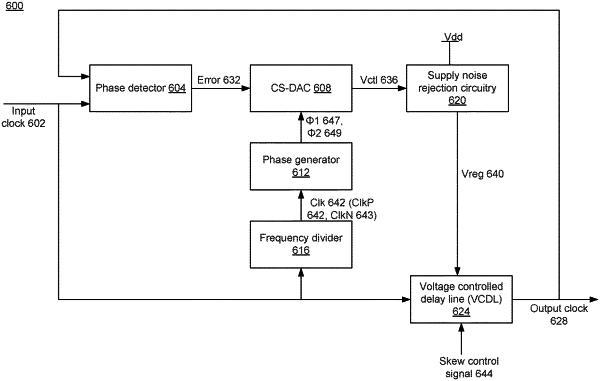
1. An apparatus, comprising:
a phase detector to receive a first clock and a second clock;
a delay line to receive the first clock and to generate the second clock, the delay line coupled to the phase detector;
a digital-to-analog converter (DAC) coupled to an output of the phase detector, wherein the DAC is to generate a control voltage at its output, the DAC comprises a multiplexer controllable by the output of the phase detector, the multiplexer is to provide one of a high or low logic level at its output according to the output of the phase detector, and the output of the multiplexer is coupled to the output of the DAC by a switched path; and
a power supply noise rejection circuitry coupled to a power supply node, wherein the power supply noise rejection circuitry is to receive the control voltage and generate a regulated voltage to control a delay of the delay line.
|