| CPC H03H 9/25 (2013.01) [H03H 9/02574 (2013.01); H03H 9/02842 (2013.01); H03H 9/131 (2013.01); H03H 9/6406 (2013.01)] | 20 Claims |
|
1. A surface acoustic wave resonator circuit comprising:
a multilayer piezoelectric substrate including a layer of piezoelectric material having a lower surface bonded to an upper surface of a layer of a dielectric material, the dielectric material having a lower surface bonded to an upper surface of a carrier substrate;
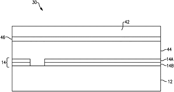
a dual-mode surface acoustic wave (DMS) resonator including a plurality of pairs of interleaved interdigital transducer (IDT) electrodes disposed on the multilayer piezoelectric substrate between first and second reflector electrode structures, each pair of interleaved IDT electrodes including a signal IDT electrode and a grounded IDT electrode, IDT electrodes of each of the plurality of pairs of IDT electrodes of the DMS resonator including an upper layer and a lower layer, the upper layer formed of a material having a higher conductivity than the lower layer, the lower layer formed of a material having a higher density than the upper layer; and
a surface acoustic wave (SAW) resonator having an output electrically coupled to an input signal electrode of the DMS resonator, the SAW resonator including interleaved IDT electrodes disposed on the multilayer piezoelectric substrate between third and fourth reflector electrode structures, the IDT electrodes of the SAW resonator each including an upper layer and a lower layer, the upper layer formed of a material having a higher conductivity than the lower layer, the lower layer formed of a material having a higher density than the upper layer.
|