| CPC H03H 7/0115 (2013.01) [H01F 27/2804 (2013.01); H01F 27/40 (2013.01); H01G 4/30 (2013.01); H01G 4/40 (2013.01); H01F 2027/2809 (2013.01); H03H 2001/0085 (2013.01)] | 11 Claims |
|
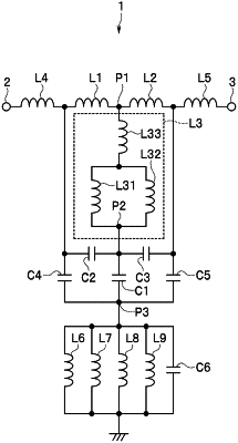
1. A multilayered low-pass filter comprising:
a first inductor and a second inductor connected in series;
a third inductor provided between a connection point of the first inductor with the second inductor and a ground in a circuit configuration;
a capacitor connected to the third inductor; and
a stack including a plurality of dielectric layers and a plurality of conductor layers stacked together, the stack being intended to integrate the first inductor, the second inductor, the third inductor, and the capacitor, wherein
the third inductor includes a first inductor portion and a second inductor portion connected in parallel,
the plurality of conductor layers include a first inductor-forming conductor layer, a second inductor-forming conductor layer, and a capacitor-forming conductor layer located at different positions, respectively, in a stacking direction of the plurality of dielectric layers,
the first inductor-forming conductor layer constitutes at least a part of each of the first and second inductors,
the second inductor-forming conductor layer includes a first portion constituting the first inductor portion and a second portion constituting the second inductor portion,
the capacitor-forming conductor layer constitutes a part of the capacitor,
the stack further includes at least one first through hole connecting the first inductor-forming conductor layer and the second inductor-forming conductor layer, at least one second through hole connecting the first portion of the second inductor-forming conductor layer and the capacitor-forming conductor layer, and at least one third through hole connecting the second portion of the second inductor-forming conductor layer and the capacitor-forming conductor layer.
|