| CPC H03F 3/193 (2013.01) [G01N 29/022 (2013.01); H03D 7/12 (2013.01); G01N 2291/0215 (2013.01); H03F 2200/451 (2013.01)] | 20 Claims |

|
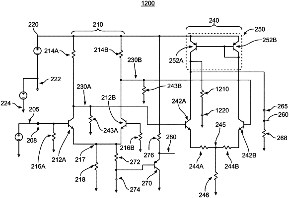
1. A limiting amplifier comprising:
a first stage, the first stage including:
a pair of first stage transistors, a first of the pair of first stage transistors adapted to receive an input voltage signal;
a first stage positive supply voltage network electrically coupled to the pair of first stage transistors; and
a first stage negative supply voltage network electrically coupled to the pair of first stage transistors;
wherein the first stage is adapted to amplify the received input voltage signal and to transmit the amplified input voltage signal as a pair of first stage output voltage signals; and
a second stage, the second stage including:
a pair of second stage transistors, each of the pair of second stage transistors adapted to receive a corresponding one of the pair of first stage output voltage signals;
an active load output circuit, the active load output circuit including:
a pair of active load transistors, each of the pair of active load transistors electrically coupled to a corresponding one of the pair of second stage transistors;
an active load impedance circuit, the active load impedance circuit including an active load feedback resistor electrically coupled between the pair of active load transistors, or an active load ground resistor electrically coupled to a first of the pair of active load transistors, the active load ground resistor optionally in series with an active load ground capacitor; and
an active load output electrically coupled to the first of the active load transistors; and
a second stage negative supply voltage network electrically coupled to the pair of second stage transistors;
wherein the second stage is adapted to amplify and voltage limit the pair of first stage output voltage signals and to transmit the amplified and voltage limited pair of first stage output voltage signals as an output voltage signal from the active load output; and
wherein an output impedance of the second stage is a function of the active load impedance circuit.
|