| CPC H03F 3/04 (2013.01) [H03K 17/687 (2013.01); H03F 1/0244 (2013.01); H03F 3/217 (2013.01); H03F 3/2171 (2013.01); H03F 2200/129 (2013.01)] | 13 Claims |
|
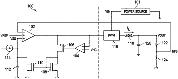
1. A device, comprising:
a capacitor;
a current source coupled to the capacitor;
at least one transistor coupled to the capacitor and configured to discharge the capacitor;
an error amplifier having first and second error amplifier inputs and an error amplifier output, wherein the first error amplifier input is coupled to the current source, the error amplifier output is coupled to the at least one transistor, and the error amplifier is configured to provide a pulse width modulation (PWM) signal at the error amplifier output; and
a clamping amplifier having a clamping amplifier input and a clamping amplifier output, wherein the clamping amplifier is configured to:
receive the PWM signal at the clamping amplifier input; and
provide a clamping signal at the clamping amplifier output responsive to the PWM signal, the clamping signal controlling the at least one transistor.
|