| CPC H02M 7/487 (2013.01) [H02M 1/084 (2013.01); H02M 1/38 (2013.01); H02M 7/53871 (2013.01)] | 20 Claims |
|
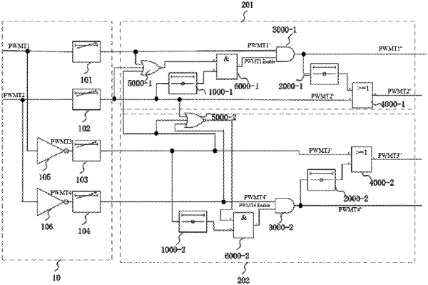
1. A control circuit for a phase bridge arm of a Neutral Point Clamp type (NPC-type) three-level converter, the phase bridge arm of the NPC-type three-level converter comprising a plurality of Insulated Gate Bipolar Transistor (IGBT) devices, the control circuit comprising:
an off-time control circuit configured to reserve a preset time period for turn-off of the plurality of IGBT devices in the phase bridge arm, wherein a set of input terminals of the off-time control circuit is configured to receive a set of Pulse Width Modulation (PWM) signals for controlling the plurality of IGBT devices; and
a timing control circuit comprising a first sub-circuit and a second sub-circuit,
wherein the first sub-circuit comprises a first fixed delay circuit, a second fixed delay circuit, a first AND gate circuit, and a first OR gate circuit,
wherein the second sub-circuit comprises a third fixed delay circuit, a fourth fixed delay circuit, a second AND gate circuit, and a second OR gate circuit,
wherein in the first sub-circuit, a first input terminal of the first AND gate circuit is connected to a first output terminal of the off-time control circuit, a second input terminal of the first AND gate circuit is connected to a second output terminal of the off-time control circuit via the first fixed delay circuit, an output terminal of the first AND gate circuit is connected to a first input terminal of the first OR gate circuit via the second fixed delay circuit, and a second input terminal of the first OR gate circuit is connected to the first output terminal of the off-time control circuit,
wherein in the second sub-circuit, a first input terminal of the second AND gate circuit is connected to a third output terminal of the off-time control circuit via the third fixed delay circuit, a second input terminal of the second AND gate circuit is connected to a fourth output terminal of the off-time control circuit, an output terminal of the second AND gate circuit is connected to a first input terminal of the second OR gate circuit via the fourth fixed delay circuit and a second input terminal of the second OR gate circuit is connected to the third output terminal of the off-time control circuit,
wherein output terminals of the timing control circuit are respectively connected to gate terminals of the plurality of IGBT devices, and
wherein the output terminal of the first AND gate circuit in the first sub-circuit, an output terminal of the first OR gate circuit in the first sub-circuit, the output terminal of the second AND gate circuit in the second sub-circuit, and an output terminal of the second OR gate circuit in the second sub-circuit serve as the output terminals of the timing control circuit, respectively.
|