| CPC H02M 1/32 (2013.01) [H03K 5/24 (2013.01); H03K 17/0822 (2013.01)] | 27 Claims |
|
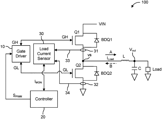
1. A gate driver system configured to drive a load, the gate driver system configured to drive a half bridge circuit comprising a high-side transistor and a low-side transistor, the gate driver system comprising:
a gate driver circuit configured to drive the high-side transistor and the low-side transistor between switching states based on at least one control signal to control a load current, wherein the load current is a positive load current when it flows towards the load and is a negative load current when it flows away from the load;
a control circuit configured to regulate the at least one control signal in response to detecting a negative load overcurrent event,
wherein the control circuit is configured to monitor for the negative load overcurrent event and detect the negative load overcurrent event in response to the load current being less than a negative overcurrent threshold, and
wherein, in response to detecting the negative load overcurrent event, the control circuit is configured to turn off the low-side transistor and turn on the high-side transistor such that the negative load current flows through a gate-controlled conductive channel of the high-side transistor.
|