| CPC H02J 50/90 (2016.02) [A61M 60/178 (2021.01); A61M 60/216 (2021.01); A61M 60/523 (2021.01); A61M 60/538 (2021.01); A61M 60/873 (2021.01); H02J 50/12 (2016.02); A61M 60/148 (2021.01); A61M 2205/04 (2013.01); A61M 2205/3515 (2013.01); A61M 2205/3523 (2013.01); A61M 2205/3561 (2013.01); A61M 2205/8243 (2013.01); H03H 7/40 (2013.01)] | 7 Claims |
|
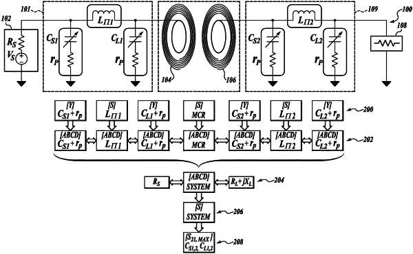
1. An adaptive impedance matching wireless power transfer system (100) comprising:
a drive inductor (103) configured to receive alternating current electric power from a power source at a fixed frequency;
a high quality factor, (high-Q), transmitter coil (104) inductively coupled to the drive inductor;
a high-Q receiver coil (106) configured to be inductively coupled to the transmitter coil; and
a first impedance matching network (101) that is operably coupled to the drive inductor and configured to selectively adjust the impedance between the drive inductor and the transmitter coil, wherein the first impedance matching network comprises a plurality of capacitors (150) interconnected to form at least one switchable bank of capacitors, and a microcontroller (154) operably connected to the at least one switchable bank of capacitors, wherein the microcontroller is configured and operable to receive a measured operating parameter of the adaptive impedance matching wireless power transfer system and to use the measured operating parameter to selectively adjust the impedance between the drive inductor and the transmitter coil,
wherein the first impedance matching network (101) comprises a first π-match network with variable capacitances comprising a switchable first bank of capacitors (150) that are connected to a switchable second bank of capacitors (152) with a π-match inductor, and further wherein the microcontroller (154) is operably connected to both the switchable first and second banks of capacitors to selectively adjust the capacitance of the first and second banks of capacitors, thereby adjusting the impedance between the drive inductor (103) and the transmitter coil (104), wherein each capacitor of the first and second switchable bank of capacitors is coupled to the microcontroller through a network of controllable micro-switches and a gate drive filter, wherein the gate drive filter (Q) comprises a first resistor that couples the gate drive filter to the microcontroller, a second resistor that couples the gate drive filter to a voltage source, a diode (D) that couples the gate driver and filter to the micro-switches and the second resistor, wherein a cathode of the diode is coupled to the gate drive filter, and an anode of the diode is coupled to the microswitches and to the second resistor.
|